Saturday, 29 September 2012

Ric Elias: 3 things I learned while my plane crashed


Ric Elias had a front-row seat on Flight 1549, the plane that crash-landed in the Hudson River in New York in January 2009. What went through his mind as the doomed plane went down? At TED, he tells his story publicly for the first time.

Ric Elias is the CEO of Red Ventures, a marketing services company that grew out of Elias' long experience in business.


Refference: TED Talk

Keith Barry: Brain Magic

                                                   
First, Keith Barry shows us how our brains can fool our bodies -- in a trick that works via podcast too. Then he involves the audience in some jaw-dropping (and even a bit dangerous) feats of brain magic.
       Think of Keith Barry as a hacker of the human brain -- writing routines that exploit its bugs and loopholes, and offering a revealing look at the software between our ears.


Refference: TED Talk

Thursday, 27 September 2012

Cockroaches controlled by remote control: A search-and-rescue


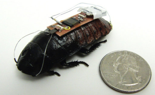
Researchers say they've figured out a way to create cyborg, remote-controlled cockroaches, hoping one day the resilient creatures could be steered into disaster zones to gather information and look for survivors.
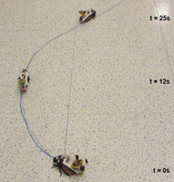
Video footage from the experiments at North Carolina State University shows the part-robot roaches being directed along a curving path via remote control. The researchers say they attached a lightweight chip with a wireless receiver and transmitter onto Madagascar hissing cockroaches and wired a microcontroller to the insects' antennae and cerci — the sensory organs on the bug's abdomen that cause it to run away from danger.

Cyborg Cockroaches May Be Future Emergency Responders            Cyborg Cockroaches May Be Future Emergency Responders

With electrical signals, the researchers stimulated the cerci to trick the roaches into thinking they needed to scamper away from a predator. Once moving, charges sent to the antennae controlled the insects' direction. A signal sent to one antenna could make a roach think its feeler was touching a wall, sending it in the opposite direction, a statement from NC State explained.
"Building small-scale robots that can perform in such uncertain, dynamic conditions is enormously difficult. We decided to use biobotic cockroaches in place of robots, as designing robots at that scale is very challenging, and cockroaches are experts at performing in such a hostile environment," NC State researcher Alper Bozkurt said in the statement.


"Ultimately, we think this will allow us to create a mobile web of smart sensors that uses cockroaches to collect and transmit information, such as finding survivors in a building that's been destroyed by an earthquake," Bozkurt added.
The researchers reported the results of their experiments late last month at the annual International Conference of the IEEE Engineering in Medicine & Biology Society in San Diego, Calif.
Other researchers have floated the possibility of technologically enhanced roaches. Scientists at Case Western Reserve University demonstrated how the insects could be outfitted with an implantable biofuel cell powered by a sugar the bugs make from their food. Electricity from such a cell then could be used to power sensors on the insect or to manipulate it by remote control.

VeRY IntEReStINg UNKnOWn FactS

Here are some interesting, but true facts, that you may or may not have known.


1. The Statue of Liberty's index finger is eight feet long.
2. Rain has never been recorded in some parts of the Atacama Desert in Chile.
3. A 75 year old person will have slept about 23 years.
4. Boeing 747's wing span is longer than the Wright brother's first flight. The Wright brother's invented the airplane.
5. There are as many chickens on earth as there are humans.
6. One type of hummingbird weighs less than a penny.
7. The word "set" has the most number of definitions in the English language; 192 Slugs have four noses.
8. Sharks can live up to 100 years.
9. Mosquitos are more attracted to the color blue than any other color.
10. Kangaroos can't walk backwards.
11. About 75 acres of pizza are eaten in in the U.S. everyday.
12. The largest recorded snowflake was 15 Inch wide and 8 Inch thick. It fell in Montana in 1887.
13. The tip of a bullwhip moves so fast that the sound it makes is actually a tiny sonic boom.
14. Former president Bill Clinton only sent 2 emails in his entire 8 year presidency.
15. Koalas and humans are the only animals that have finger prints.
16. There are 200,000,000 insects for every one human.
17. It takes more calories to eat a piece of celery than the celery had in it to begin with.
18. The world's largest Montessori school is in India, with 26,312 students in 2002.
19. Octopus have three hearts.
20. If you ate too many carrots, you would turn orange.
21. The average person spends two weeks waiting for a traffic light to change.
22. 1 in 2,000,000,000 people will live to be 116 or old.
23. The body has 2-3 million sweat glands.
24. Sperm whales have the biggest brains; 20 lbs.
25. Tiger shark embroyos fight each other in their mother's womb. The survivor is born.
26. Most cats are left pawed.
27. 250 people have fallen off the Leaning Tower of Pisa.
28. A Blue whale's tongue weighs more than an elephant.
29. You use 14 muscles to smile and 43 to frown. Keep Smiling!
30. Bamboo can grow up to 3 ft in 24 hours.
31. An eyeball weighs about 1 ounce.

Wednesday, 30 May 2012

Embedded systems (Video tutorials)


Lecture -1: Introduction


Lecture-2: Embedded Hardware


Lecture 3: Instruction Set


Lecture 4: Peripherals on Chip


Lecture 5: ARM processor


Lecture 6: ARM instuctions


Lecture 7:ARM-Interrupt processing

Friday, 23 March 2012

SIXTH SENSE TECHNOLOGY

Sixth Sense Technology is a mini- projector coupled with  a camera    and   a Cell phone—which acts as the   computer and     connected to the    Cloud, all the information   stored   on the   web. Sixth Sense can also obey hand   gestures. The Camera   recognizes  objects  around a person instantly, with t   he micro projector Overlaying the  information    on   any surface, including the object itself or hand.


  Also can access or manipulate   the information using fingers.  Make a call by Extend hand on front of the projector and   numbers   will appear for   to click. Know the time by Draw a circle on   wrist and a watch will appear. take a   photo  by Just make a square with fingers, highlighting what want to frame, and the  system will make  the    photo     which   can  later organize  with the others using own hand   over  the air. and The device has a  huge  number of applications ,it is portable and easily  to  carry  as  can   wear    it  in neck. The drawing   application     lets user draw On any surface by observe   the     movement of index    finger.


 Mapping can also be done   any where with the features    of zooming in or zooming out. The camera also helps   user to take pictures   of   the scene is viewing and later can arrange them on any surface. Some of the   more practical uses are reading   a   newspaper. Reading   a newspaper rand viewing videos instead of the photos in the   paper. Or live sports     up dates   while    reading    the newspaper. The device can also tell arrival, departure or delay time of air plane on tickets. For book lovers it is nothing less than a blessing. Open any book and find the amazon ratings of the book. To add to it, pick any page and the device gives additional information on the text, comments and   lot       more   add on feature.

For more info, watch dis video...

Wednesday, 21 March 2012

Types of Soldering & Soldering Process


What is Soldering?
Soldering - a must skill for all electrical and electronic works. “Soldering” is defined as the process of joining two pieces of metals using a filler metal, known as solder, having a low melting point below the melting point of the work piece. It is often confused with welding but the difference between them is, in soldering the work piece is not melted, they are joined using a filler metal, but in welding work piece is joined by melting.
History
Soldering was practiced as far back as 5000 years ago in Egypt. Soldering was widely performed around 4000 years ago when tin was discovered as soldering metal. The process of soldering was introduced in Mediterranean region, and was followed in the Roman Empire, Swiss and Hungaria. Soldering has improved a lot from culture to culture and generation to generation and in today’s scenario it is the best method for fabrication and assembly of microelectronics.

Types of Soldering
Soldering is classified as shown in the image below:

1.  Soft soldering
It is a process for joining small intricate parts having low melting points which damages when soldering process is carried out at high temperature. It uses tin-lead alloy as filler material. The melting point of the filler material should be below 400oC (752oF). It uses gas torch as the heat source.


2.  Hard soldering
In this process, hard solder connects two pieces of metals by expanding into the pores of the work piece opened by high temperature. The filler material possess high temperature above 450oC (840oF).


It comprises of two parts namely silver soldering and brazing.
2.1  Silver soldering
It is a clean process useful for fabricating small fittings, doing odd repairs and making tools. It uses an alloy containing silver as filler material. Silver provides free flowing characteristics but silver solder is not good at gap filling hence, different fluxes are recommended for precised silver solder.


2.2  Brazing
Brazing is a process of joining two pieces of base metals by creating melted metallic filler that flows by capillary attraction across the joints and cools to form a solid bond through atomic attraction and diffusion. It creates an extremely strong joint. It uses brass alloy as filler material.

SOLDER
 It is any of various fusible alloys usually tin or lead used to join metallic parts. It is symbolized by two numbers which represents the percentage of each metal in a mixture. The first number refers to the percentage of tin and second to the percentage of lead. It usually melts at a temperature of about 200oC. Since solder has tin content, coating a surface with solder is called “tinning”.

Types of solder
·         60/40 solder- its composition is 60% tin and 40% lead. It melts at 374oF. It forms high, rounded, beaded seams. Because of its low relatively melting point this type of solder is easy to rework to maintain a smooth finish.
·         50/50 solder- its composition is 50% tin and 50% lead. Its melting point is 421oF. This type of solder produces a much flatter bead than 60/40. Because of its high melting point this type of solder is often used on the back of stained glasses, to protect it from melting when soldering the front.
·         63/37 solder- its composition is 63% tin and 37% lead. This type of solder is an excellent solder to bead up the outside rim of copper foiled pieces. It is often referred as decorated or quick set solder.
·         Lead free solder- This type of solder performs similar to 50/50 solder. Lead free solder is a most expensive solder, but when constructing pieces that will contact food or that are handled frequently, this type of solder is different.

The best size of solder for electronic circuit board is 22swg (SWG=standard wire gauge). Solder for electronic use contains tiny cores of flux. Without flux most joints would fail because metals quickly oxidize and the solder itself will not flow properly.
Now the question arises, why solder method is preferred over other bonding methods?
Since low energy is required to solder, it is relatively inexpensive and easy to use. If the joints are properly soldered they are highly reliable and can last for years decade and centuries. In addition to this, solder joints are easy to repair.
Process of soldering
The basic soldering operation is performed in the following steps:
Cleaning - Heated metal are prone to oxidize rapidly. That is why oxides, scale and dirt must be removed by chemical or mechanical actions. Hence, initially, we check the tip of the soldering iron which should be clean and shiny, suitable for the project to be carried out. If not, then to fulfill the requirements of the project, small amount of the solder is added on the tip of the iron.


For effective cleaning of the tip of soldering iron, one should ensure that the sponge used for the same should be damped. As a dry sponge will not clean the tip effectively, and a wet sponge will lower the temperature of the tip making for an ineffective solder joint.

Heating- The temperature of the soldering station should be adjusted to a considerable level of 350oC, so as to achieve the required melting conditions of the alloy used for soldering.
Insertion- Further, the components which are to be soldered, are inserted in the holes of the circuit board by bending the lead using fine pliers, so that they can slide easily in the holes provided on the printed circuit pad. Then the leads protruding from the bottom of the circuit board, is bend at an angle of approx 45o.
Cut off the leads of the component which are close to the outer edge of the solder pad.

Soldering - the lead and the pad are heated simultaneously, holding the soldering iron at an angle of 45o and keeping the solder wire in contact to the space between the iron tip and lead. As the solder melts around the joints, the soldering wire should be kept still for good results. And remove the solder tip first and the solder wire next.
After soldering the joint, instead of blowing off the solder joint, allow it to cool naturally.

Removal of residue- Using isopropyl alcohol, and a bristle brush the printed circuit board should be cleaned thoroughly after the soldering of the components is completed. This process removes the flux residue and the unwanted contaminations present on the circuit board. If any of the flux remains, it’ll continue to react with the solder, causing oxidation. Therefore, this step is very important.

Finishing - finishing wax is used after cleaning process for enhancing the color of the patina making it either rich black or shinny copper and to keep it looking it’s best. Apply the patina to the solder lines using a cotton swab.


Types of Soldering Processes:
Wave Soldering
It is one of the primary techniques of soldering in which electronic components are soldered to a printed circuit boards. A solder wave is created by a pump located at the bottom of the solder pot. Components are inserted into the holes and the loaded PCB is placed onto a conveyer, which brings it into the contact with the wave surface. The solder wets the metallic area on the board, creating electrical and mechanical connections. The wave soldering technique encompasses a sequence of process, all of which are contained in same apparatus. First of all, the surface is coated with flux. After the flux is applied, the substrate is passed through a preheating stage which promotes the activation of flux, evaporates the volatiles of flux and reduces the thermal shock to the substrate and devices when it passes onto the solder wave. After this, surface board passes from the solder wave and leads to formation of joints. After passing the solder wave, the board cools through natural heat loss.
Reflow Soldering
Reflow soldering is a widely spread technology of soldering of surface mount semiconductor packages. The reflow process consist of applying a eutectic solder paste to a circuit board, placing devices onto the plate, and then conveying the board through a reflow oven or under an infrared lamp or by using hot air pencil, with successive heating elements of varying temperature. When the entire assembly is subjected to controlled heat, solder melts and the joint is permanently connected.
FLUX
Soldering flux is formulated to remove a film of oxides from the metal and make the solder and the metal more able to dissolve in each other. Flux must be able to deoxidize metal surfaces at high temperatures without decomposing. The flux material simultaneously reduce the surface tension of the flowing solder and in this way, brings about better wetting characteristics and a more favorable flowing property.


Rosin flux
 It is the oldest, most popular and still the most effective soldering flux. Rosin, which is the base of this type of flux, is extracted from pine trees. The active agents in rosin flux are abeitic acid and plicatic acid; it is the reaction between these acids and the metallic oxides on the joint materials that provides the cleaning required for wetting the joint. After soldering, rosin based flux leaves behind the residue which is non-corrosive, non conducting, moisture and fungus resistant but it must be cleaned from the surface before carrying any further process to minimize fuss and irritation in eyes and skin caused by combustion.

Water soluble fluxes
These are the fluxes that wash away when the board is washed with the ordinary water mainly hot water. Occasionally, all the water soluble flux leaves behind residues. These are carboxylic acids and detergent which produces irritating fumes. Hence, in addition to hot water saponifier is added to help the cleaning process. Saponifiers are alkaline and may be corrosive; they react with acid residue on board to form soap and glycerin, which is relatively easy to wash with hot water. If adequate cleaning of the residues is not carried then they may cause sustained corrosion and induces electrical problems.

No clean fluxes
These fluxes leave minimal residues which need not be removed after soldering from finished electronic assemblies. They vanish under the influence of heat. Many no-clean fluxes are organically based, usually on an alcohol, and have a low solid content. Some water based no-clean fluxes have been developed but these must be handled with care to avoid severe skin irritation. No-clean fluxes have been found to be even more irritating than rosin fluxes. Fluxes must react with the pad material to be effective and enhance wetting; the acids in these fluxes do that, but chemical reactions with the metals in the pads and the plastic substrate produce very harsh gases.
Desoldering
The reverse process of soldering is desoldering. It is a process of removal of solder and components mounted on circuit boards for repair purpose.

What if a soldering is not done properly? How to resolve this problem? Simply, the soldered joint is removed by the process of desoldering. For this purpose a vacuum pump is activated to remove solder from the plated through holes. The lead over which the desoldering tip was placed is moved in a circular motion for rounded leads and back and forth for flat leads.


Applications
Soldering has the most common use in plumbing and in the field of electronics where it is used to mount electronic components on printed circuit boards. In addition to this, soldering has its application in jewellary making, cooking wares, tools, stained glass work and many more. It can also be used to repair a leakage in containers.


Tuesday, 20 March 2012

Understanding touchscreen technology


Touchscreens (sometimes spelled as touch screen) are everywhere: they are embedded in phones, office equipment, speakers, digital photo frames, TV control buttons, remote controls, GPS systems, automotive keyless entry, and medical monitoring equipment. As a component, they have reached into every industry, every product type, every size, and every application at every price point. In fact, if a product has an LCD or buttons, a designer somewhere is probably evaluating how that product, too, can implement touchscreen technology. As with any technology, there are many different ways to implementation approaches, many promises of performance, and many different technical considerations when designing a touchscreen.
Anatomy of a touchscreen
Knowing what you need is an important first step in designing a touchscreen product. Vendors in the touchscreen supply chain frequently offer different pieces of the puzzle, often times combining several to create a value chain for the end customer. Figure 1 shows a blowup of the touchscreen ecosystem. This ecosystem is the same whether it is in the latest Notebook PC or the latest touch-enabled mobile phone.

Figure 1: Touchscreen contoller "autopsy"
  
 There are six key elements:
1. Front panel or bezel: The front panel or bezel is the outermost skin of the end product. In some products, this bezel will encompass a protective clear overlay to keep weather and moisture out of the system, and to resist scratching and vandalism to the underlying sensor technology (see item 3 below). Other times, the outmost bezel simply covers the edges of the underlying touch sensor; in this case, it is purely decorative.
2. Touch controller: The touch-controller is generally a small microcontroller-based IC that sits between the touch sensor and the embedded system controller. This IC can either be located on a controller board inside the system or it can be located on a flexible printed circuit (FPC) affixed to the glass touch sensor. This touch controller takes information from the touch sensor and translates it into information that the PC or embedded system controller can understand.
3. Touch sensor: A touchscreen "sensor" is a clear glass panel with a touch-responsive surface. This sensor is placed over an LCD so that the touch area of the panel covers the viewable area of the video screen. There are many different touch-sensor technologies on the market today, each using a different method to detect touch input. Fundamentally, these technologies all use an electrical current running through the panel that, when touched, causes a voltage or signal change. This voltage change is sensed by the touch controller to determine the location of the touch on the screen.
4. Liquid crystal display: Most touchscreen systems work over traditional LCDs. LCDs for a touch-enabled product should be chosen for the same reasons they would in a traditional system: resolution, clarity, refresh speed, and cost. One major consideration for a touchscreen, however, is the level of electrical emission. Because the technology in the touch sensor is based on small electrical changes when the panel is touched, an LCD that emits a lot of electrical noise can be difficult to design around. Touch sensor vendors should be consulted before choosing an LCD for a touchscreen system.
5. System software : Touchscreen driver software can be either shipped from the factory (within the embedded OS of a cell phone) or offered as add-on software (like adding a touchscreen to a traditional PC). This software allows the touchscreen and system controller to work together and tells the product's operating system how to interpret the touch-event information that is sent from the controller. In a PC-style application, most touchscreen drivers work like a PC mouse. This makes touching the screen similar to clicking the mouse at the same location on the screen. In embedded systems, the embedded controller driver must compare the information presented on the screen to the location of the received touch.
The "big three" of touchscreen technology
Resistive touchscreens are the most common touchscreen technology. They are used in high-traffic applications and are immune to water or other debris on the screen. Resistive touchscreens are usually the lowest-cost touchscreen implementation. Because they react to pressure, they can be activated by a finger, gloved hand, stylus, or other object, such as a credit card.
Surface-capacitive touchscreens provide a much clearer display than the plastic cover typically used in a resistive touchscreen. In a surface-capacitive display, sensors in the four corners of the display detect capacitance changes due to touch. These touchscreens can only be activated by a finger or other conductive object.
Projected-capacitive touchscreens are the latest entry to the market. This technology also offers superior optical clarity, but it has significant advantages over surface-capacitive screens. Projected capacitive sensors require no positional calibration and provide much higher positional accuracy. Projected-capacitive touchscreens are also very exciting because they can detect multiple touches simultaneously.
How touchscreens work
Let's look inside the two most common touchscreen technologies.
The most widely used touchscreen technology is resistive. Most people have used one of these resistive touchscreens already, in the ATM at the bank, in the credit card checkout in most stores, or even for entering an order in a restaurant. Projective-capacitance touchscreens, on the other hand, are not as broadly available yet, but are gaining market momentum. Many cellphones and portable music players are beginning to come to market with projective-capacitance interfaces. Both resistive and capacitive technologies have a strong electrical component, both use ITO (Indium-Tin-Oxide, a clear conductor), and both will be around for a long time to come.
A resistive touchscreen (Figure 2, left side) consists of a flexible top layer, then a layer of ITO (Indium-Tin-Oxide), an air gap and then another layer of ITO. The panel has 4 wires attached to the ITO layers: one on the left and right sides of the 'X' layer, and one on the top and bottom sides of the 'Y' layer.

Figure 2. Stackup layers for "resistive" (left) and "capacitive" (right) screens

A touch is detected when the flexible top layer is pressed down to contact the lower layer. The location of a touch is measured in two steps: First, the 'X right' is driven to a known voltage, and the 'X left' is driven to ground and the voltage is read from a Y sensor. This provides the X coordinate. This process is repeated for the other axis to determine the exact finger position.
Resistive touchscreens also come in 5-wire, and 8-wire versions. The 5-wire version replaces the top ITO layer with a low-resistance "conductive layer" that provides better durability. The 8-wire panel was developed to enable higher resolution by enabling better calibration of the panel's characteristics.
There are several drawbacks to resistive technology. The flexible top layer has only 75%-80% clarity and the resistive touchscreen measurement process has several error sources. If the ITO layers are not uniform, the resistance will not vary linearly across the sensor. Measuring voltage to 10- or 12-bit precision is required, which is difficult in many environments. Many of the existing resistive touchscreens also require periodic calibration to realign the touch points with the underlying LCD image.
Conversely, projected-capacitive touchscreens have no moving parts. The only thing between the LCD and the user is ITO and glass, which have near 100% optical clarity. The projected-capacitance sensing hardware consists of a glass top layer (Figure 2, right side), followed by an array of X sensors, an insulating layer, then an array of Y sensors on a glass substrate. The panel will have a wire for each X and Y sensor, so a 5 x 6 panel will have 11 connections (Figure 3), while a 10 x 14 panel will have 24 sensor connections.
Figure 3. Signal intensity at rows and columns denote location of touch

As a finger or other conductive object approaches the screen, it creates a capacitor between the sensors and the finger. This capacitor is small relative to the others in the system (about 0.5 pF out of 20 pF), but it is readily measured. One common measuring technique known as Capacitive Sensing using a Sigma-Delta Modulator (CSD) involves rapidly charging the capacitor and measuring the discharge time through a bleed resistor.
A projected capacitive sensor array is designed so that a finger will interact with more than one X sensor and more than one Y sensor at a time (See Figure 3). This enables software to accurately determine finger position to a very fine degree through interpolation. For example, if sensors 1, 2 and 3 see signals of 3, 10, and 7, the center of the finger is at:
[(1 × 3) + (2 × 10) + (7 × 3)]/(3 + 10 + 7) = 2.2

Since projected-capacitive panels have multiple sensors, they can detect multiple fingers simultaneously, which is impossible with other technologies. In fact, projective capacitance has been shown to detect up to ten fingers at the same time. This enables exciting new applications based on multiple finger presses, including multiplayer gaming on handheld electronics or playing an touchscreen piano.
Without question, touchscreens are great looking. They have begun to define a new user interface and industrial design standard that is being adopted the world over. In everything from heart-rate monitors to the latest all-in-one printers, touchscreens are quickly becoming the standard of technology design.
Beyond just looks, however, touchscreens provide an unparalleled level of security from tampering, resistance from weather, durability from wear, and even enable entirely new markets with unique features such as multi-touch touchscreens. With touchscreens making their way into so many types of products, it's imperative that design engineers understand the technology ecosystem and technology availability.


Tuesday, 13 March 2012

How to make a PCB at home


Often people face problem while making a circuit on a bread board. It is a common problem that the circuit may work some time and may not work other time. Most of the time it is the connections on the bread board which creates this problem. Either are connections are not proper or loose or may get damaged while working or carrying the circuit on a bread board. Hence it is always recommended to make the circuit on a PCB once it has been tested on a bread board. This article will explain the process of making a single layer PCB at home with the use of commonly available tools.

A printed circuit board has pre-designed copper tracks on a conducting sheet. The pre-defined tracks reduce the wiring thereby reducing the faults arising due to lose connections. One needs to simply place the components on the PCB and solder them.

Materials required:
•         Over Head Projector sheet (known as OHP sheets) or a wax paper.
•         Laser Printer.
•         Electric Iron.
•         Steel wool.
•         Two plastic trays.
•         Copper board/ PCB (eg: paper phenolic, glass epoxy, FR4, FR10, etc.)
•         Black permanent marker.
•         Etching solution (Ferric chloride).
•         Drill machine.

Step 1: Prepare a layout of the circuit on any commonly used PCB designing software. A layout is a design which interconnects the components according to the schematic diagram (circuit diagram). Take a mirror image print of the layout on the OHP sheet using a laser printer. Make sure that the design is correct with proper placement of the components.
Step 2: Cut the copper board according to the size of layout. A copper board is the base of a PCB, it can be single layer, double layer or multi layer board.
Single layer copper board has copper on one side of the PCB, they are used to make single layer PCBs, it is widely used by hobbyist or in the small circuits. A double layer copper board consists of copper on both the sides of the PCB. These boards are generally used by the industries. A multilayer board has multiple layers of copper; they are quite costly and mainly used for complex circuitries like mother board of PC.
Step 3: Rub the copper side of PCB using steel wool. This removes the top oxide layer of copper as well as the photo resists layer if any.
Step 4: Place the OHP sheet (wax paper) which has the printed layout on the PCB sheet. Make sure that the printed/mirror side should be placed on the copper side of PCB.
 Step 5: Put a white paper on the OHP sheet and start ironing. The heat applied by the electric iron causes the ink of the traces on the OHP sheet to stick on the copper plate exactly in the same way it is printed on the OHP sheet. This means that the copper sheet will now have the layout of the PCB printed on it. Allow the PCB plate to cool down and slowly remove the OHP sheet. Since it is manual process it may happen that the layout doesn’t comes properly on PCB or some of the tracks are broken in between. Use the permanent marker and complete the tracks properly.
Step 6: Now the layout is printed on PCB. The area covered by ink is known as the masked area and the unwanted copper, not covered by the ink is known as unmasked area. Now make a solution of ferric chloride. Take a plastic box and fill it up with some water. Dissolve 2-3 tea spoon of ferric chloride power in the water. Dip the PCB into the Etching solution (Ferric chloride solution, Fecl3) for approximately 30 mins. The Fecl3 reacts with the unmasked copper and removes the unwanted copper from the PCB. This process is called as Etching.  Use pliers to take out the PCB and check if the entire unmasked area has been etched or not. In case it is not etched leave it for some more time in the solution. 
Step 7: Take out the PCB wash it in cold water and remove the ink by rubbing it with steel wool. The remaining area which has not been etched is the conductive copper tracks which connect the components as per the circuit diagram.

 Step 8: Now carefully drill the PCB using a drilling machine on the pads.
                                      
 Step 9: Put the components in the correct holes and solder them.

This completes your PCB fabrication now put the components on mounting side and solder them. Make sure that you properly dispose of the FeCl3 solution, clean your tools and wash your hands after this exercise. You can also store the solution in a plastic box for future use but not for too long.


LIFI- a new technology


Whether you’re using wireless internet in a coffee shop, stealing it from the guy next door, or competing for bandwidth at a conference, you’ve probably gotten frustrated at the slow speeds you face when more than one device is tapped into the network. As more and more people—and their many devices—access wireless internet, clogged airwaves are going to make it increasingly difficult to latch onto a reliable signal.

But radio waves are just one part of the spectrum that can carry our data. What if we could use other waves to surf the internet?


One German physicist, Harald Haas, has come up with a solution he calls “data through illumination”—taking the fiber out of fiber optics by sending data through an LED lightbulb that varies in intensity faster than the human eye can follow. It’s the same idea behind infrared remote controls, but far more powerful.

Haas says his invention, which he calls D-Light, can produce data rates faster than 10 megabits per second, which is speedier than your average broadband connection. He envisions a future where data for laptops, smartphones, and tablets is transmitted through the light in a room. And security would be a snap—if you can’t see the light, you can’t access the data.

You can imagine all kinds of uses for this technology, from public internet access through street lamps to auto-piloted cars that communicate through their headlights. And more data coming through the visible spectrum could help alleviate concerns that the electromagnetic waves that come with WiFi could adversely affect your health. Talk about the bright side.

WATCH THIS VIDEO


FLICKERING lights are annoying but they may have an upside. Visible light communication (VLC) uses rapid pulses of light to transmit information wirelessly. Now it may be ready to compete with conventional Wi-Fi.
"At the heart of this technology is a new generation of high-brightness light-emitting diodes," says Harald Haas from the University of Edinburgh, UK. "Very simply, if the LED is on, you transmit a digital 1, if it's off you transmit a 0," Haas says. "They can be switched on and off very quickly, which gives nice opportunities for transmitting data."
It is possible to encode data in the light by varying the rate at which the LEDs flicker on and off to give different strings of 1s and 0s. The LED intensity is modulated so rapidly that human eyes cannot notice, so the output appears constant.
More sophisticated techniques could dramatically increase VLC data rates. Teams at the University of Oxford and the University of Edinburgh are focusing on parallel data transmission using arrays of LEDs, where each LED transmits a different data stream. Other groups are using mixtures of red, green and blue LEDs to alter the light's frequency, with each frequency encoding a different data channel.
Li-Fi, as it has been dubbed, has already achieved blisteringly high speeds in the lab. Researchers at the Heinrich Hertz Institute in Berlin, Germany, have reached data rates of over 500 megabytes per second using a standard white-light LED. Haas has set up a spin-off firm to sell a consumer VLC transmitter that is due for launch next year. It is capable of transmitting data at 100 MB/s - faster than most UK broadband connections.
Once established, VLC could solve some major communication problems. In 2009, the US Federal Communications Commission warned of a looming spectrum crisis: because our mobile devices are so data-hungry we will soon run out of radio-frequency bandwidth. Li-Fi could free up bandwidth, especially as much of the infrastructure is already in place.
"There are around 14 billion light bulbs worldwide, they just need to be replaced with LED ones that transmit data," says Haas. "We reckon VLC is a factor of ten cheaper than Wi-Fi." Because it uses light rather than radio-frequency signals, VLC could be used safely in aircraft, integrated into medical devices and hospitals where Wi-Fi is banned, or even underwater, where Wi-Fi doesn't work at all.
"The time is right for VLC, I strongly believe that," says Haas, who presented his work at TED Global in Edinburgh last week.
But some sound a cautious note about VLC's prospects. It only works in direct line of sight, for example, although this also makes it harder to intercept than Wi-Fi. "There has been a lot of early hype, and there are some very good applications," says Mark Leeson from the University of Warwick, UK. "But I'm doubtful it's a panacea. This isn't technology without a point, but I don't think it sweeps all before it, either."


Home